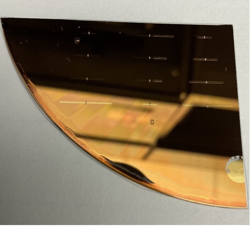
Microfabrication & MEMS

VastVision fabricates its own microscale devices in an in-house Class 5 cleanroom, spanning the full MEMS workflow: pattern, deposit, etch, and release. We combine on-site lithography and etch with partner access to national-laboratory-grade nanofabrication, so we can take a device from design through characterized hardware.

In-House Cleanroom

  • Class 5 cleanroom supporting lithography and device fabrication
  • UV lithography for micro-scale patterning
  • Plasma etching for surface treatment and pattern transfer
  • Electroplating and electrodeposition process line

MEMS Device Fabrication

  • Full pattern, deposit, etch, and release workflow
  • Thin-film sensor development
  • RF antenna and structure fabrication
  • Small-batch prototype runs with process documentation

Partner-Accessed Lithography

  • Raith Voyager electron-beam lithography
  • Raith Pioneer Two electron-beam lithography
  • JEOL JBX-8100FS electron-beam lithography
  • Class-100 photolithography via UNM and Sandia/CINT

Engagement Models

  • Prototype fabrication: design, fab, and characterize
  • Fee-for-service fabrication and tool time
  • Process development for a specific device or material
  • SBIR/STTR and sponsored research (NAICS 541715)

Nanofabrication beyond our in-house tools is available through user agreements with the Center for Integrated Nanotechnologies (CINT), the University of New Mexico, and NM Tech.