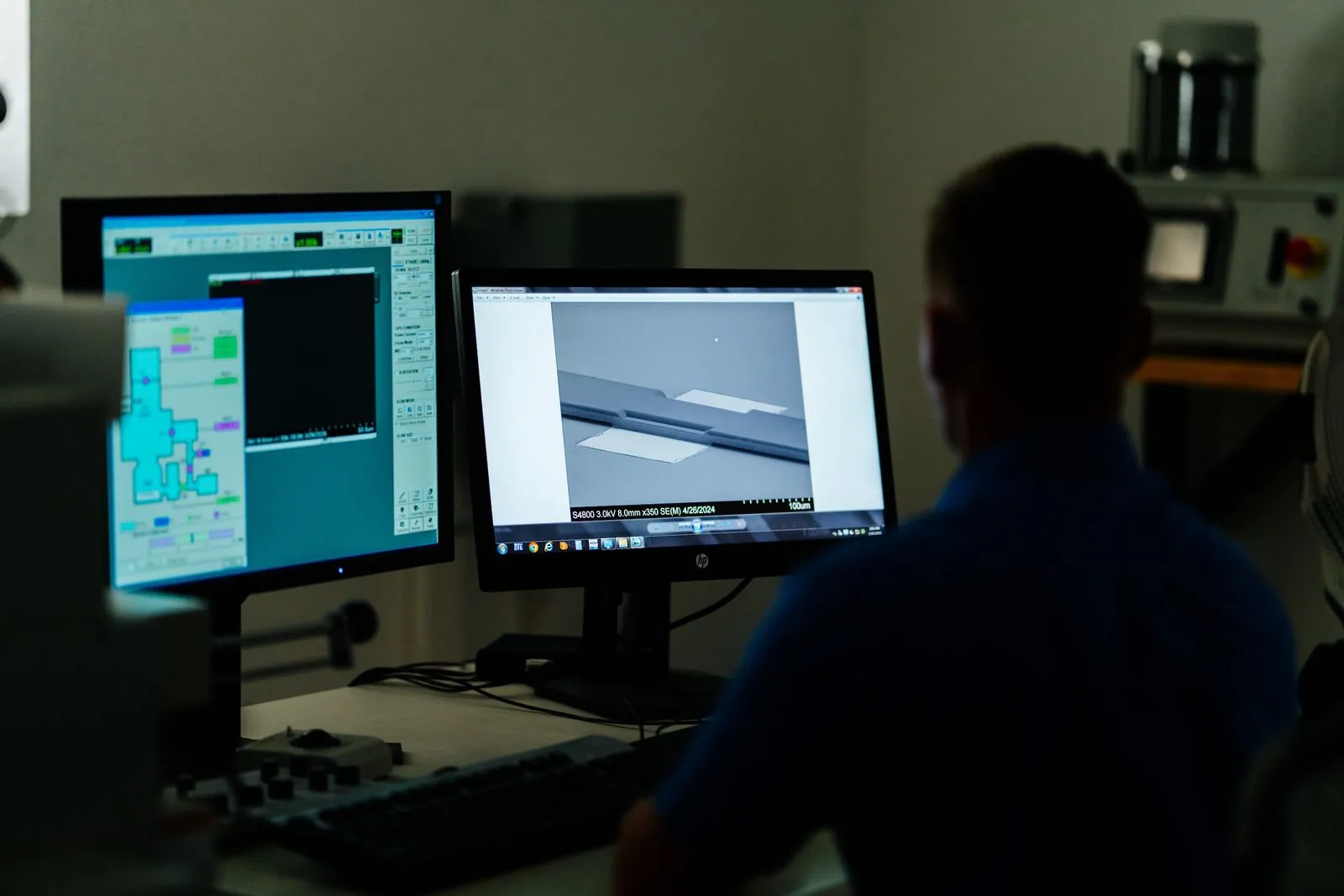
Magnetostrictive Thin Films by Aqueous Electrodeposition
A MEMS-compatible NiFeCo-Lanthanide alloy achieving greater than 700 ppm magnetostriction, deposited conformally on any geometry from aqueous solution.
Lanthanide alloys, deposited from water
VastVision has developed an aqueous electrodeposition process for NiFeCo-Lanthanide alloys, achieving greater than 700 ppm magnetostriction in a MEMS-compatible thin film.
Codepositing lanthanides at these levels was previously achievable only in non-aqueous molten-salt systems. Moving it into standard aqueous solution means the material can be built with the same electrodeposition infrastructure already used in MEMS fabrication.
Because it is plated rather than sputtered, the alloy deposits conformally on complex 3D geometries, inside channels, and on curved surfaces. It is not limited to flat substrates.
Where the alloy sits against fielded magnetostrictive materials
VastVision values are internally characterized. Wafer-scale uniformity is a program objective.
| Material | Magnetostriction | Process | Geometry constraint | MEMS |
|---|---|---|---|---|
| Metglas 2605SA1 | 15 to 25 ppm | Extruded ribbon, cut-and-place | Flat only | No |
| Galfenol (sputtered) | ~70 ppm | Sputtering | Line-of-sight, <1 µm | Limited |
| Terfenol-D (bulk) | ~2000 ppm | Directional solidification | Bulk only, brittle | No |
| VastVision NiFeCo-Ln | >700 ppm | Aqueous electrodeposition | Non-line-of-sight, any geometry | Yes |
Five decades of magnetostrictive programs across the services
| Program | Era | Material | Demonstrated |
|---|---|---|---|
| Naval Ordnance Lab / Navy | 1970s | Terfenol-D | ~2000 ppm; sonar >210 dB per transducer |
| Ames Laboratory / Navy | 1980s | Terfenol-D | Commercial production |
| DARPA CHAP / Moog | 2000s | Terfenol-D | 300 W; 60% electromechanical coupling |
| DARPA SAMPSON | 2000s | Magnetostrictive actuators | Full-scale F-15 inlet; submarine demonstration |
| NSWC Carderock / ONR | 1999 onward | Galfenol | ~70 ppm thin film; ductile; weldable |
Same physics, chip-scale form factor
Sonar & acoustic systems
Today: Terfenol-D bulk transducers. With VastVision thin films: thin-film elements for miniaturized and distributed sonar arrays.
Smart structures & SHM
Today: Metglas ribbon, bonded after fabrication. With VastVision thin films: sensing elements deposited during fabrication, not bonded after.
Shielded-facility sensing
Today: no passive route through conductive shielding. With VastVision thin films: batteryless near-field sensing through shielding, with no penetrations or wires.
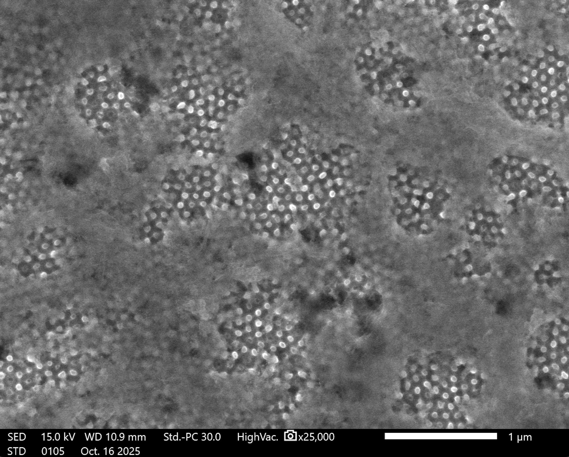
Nanowire arrays, grown in templates we make in-house
We fabricate our own anodized-alumina (AAO) templates: aluminum anodized into a dense, ordered array of nanoscale pores. The magnetostrictive alloy is then electrodeposited into those pores, using the same aqueous process as our thin films, to grow uniform, aligned nanowires.
Shaped as wires rather than films, the material responds strongly along a single axis, which makes nanowire arrays a building block for compact magnetic devices.
- In-house anodized-alumina templates
- Ordered, aligned nanowire arrays
- Aqueous electrodeposition, the same process as our thin films
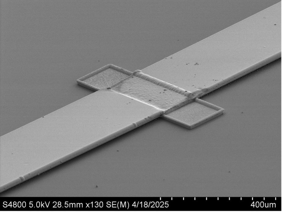
Electroplated, released, and tuned by length
The alloy is electroplated into photolithographic molds on silicon, then released from the substrate to form free-standing resonators suspended above the wafer. No out-of-plane bending is observed, because intrinsic stress is minimized during deposition.
Resonant frequency scales with 1/L, so four resonator lengths on a single chip give four sensing channels from one device, with every other material property held constant.
- Multi-frequency resonator arrays on a single wafer
- ~58 kHz baseline resonance
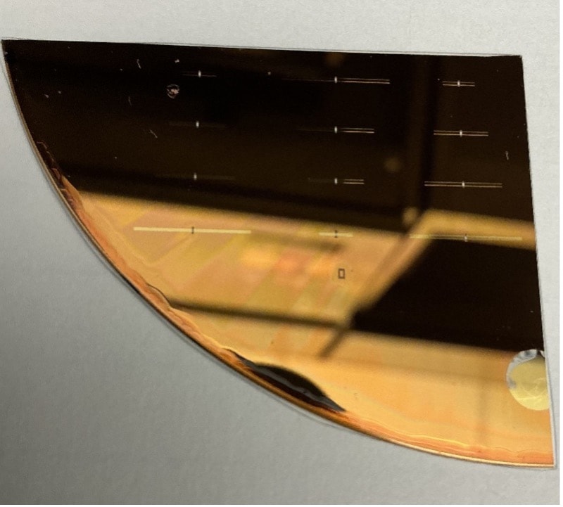
Environmental sensing by mass-loading the resonator
Adsorbed mass on the resonator surface shifts its resonant frequency. A selective coating captures a target analyte, and the frequency and amplitude shifts become the detection variables.
Hydrogen sensing was demonstrated with palladium thin films, which absorb roughly 900 times their own volume in hydrogen. Full sensor regeneration to baseline was confirmed with a nitrogen purge. Selective adsorbents for hydrogen sulfide have been identified, with experimental validation pending.
Source: TRGR Report, Sandia National Laboratories.
- Hydrogen (H₂): demonstrated
- Hydrogen sulfide (H₂S): explored
- Multiple analytes read simultaneously from one multi-frequency chip
Communicating and sensing through a Faraday cage
Near-field quasistatic magnetic fields are not governed by the skin-depth attenuation that blocks RF and propagating electromagnetic waves in conductive enclosures.
Transmitter and receiver interact through oscillating magnetic fields in the near-field zone rather than through radiation, so the signal crosses the wall of a nuclear storage canister. Current range is near-field, on the order of feet, extendable with hybrid RFID or LoRa depending on the application.
- Chipless unique identifier
- Temperature
- Tamper detection
- Pressure
- Gas sensing
- Biological agents
Co-inventors of the foundational Sandia patents
Both are named co-inventors on the foundational Sandia magnetostrictive-resonator patents. Between them they bring 39 years at Sandia National Laboratories and inventorship of 13 issued U.S. patents.
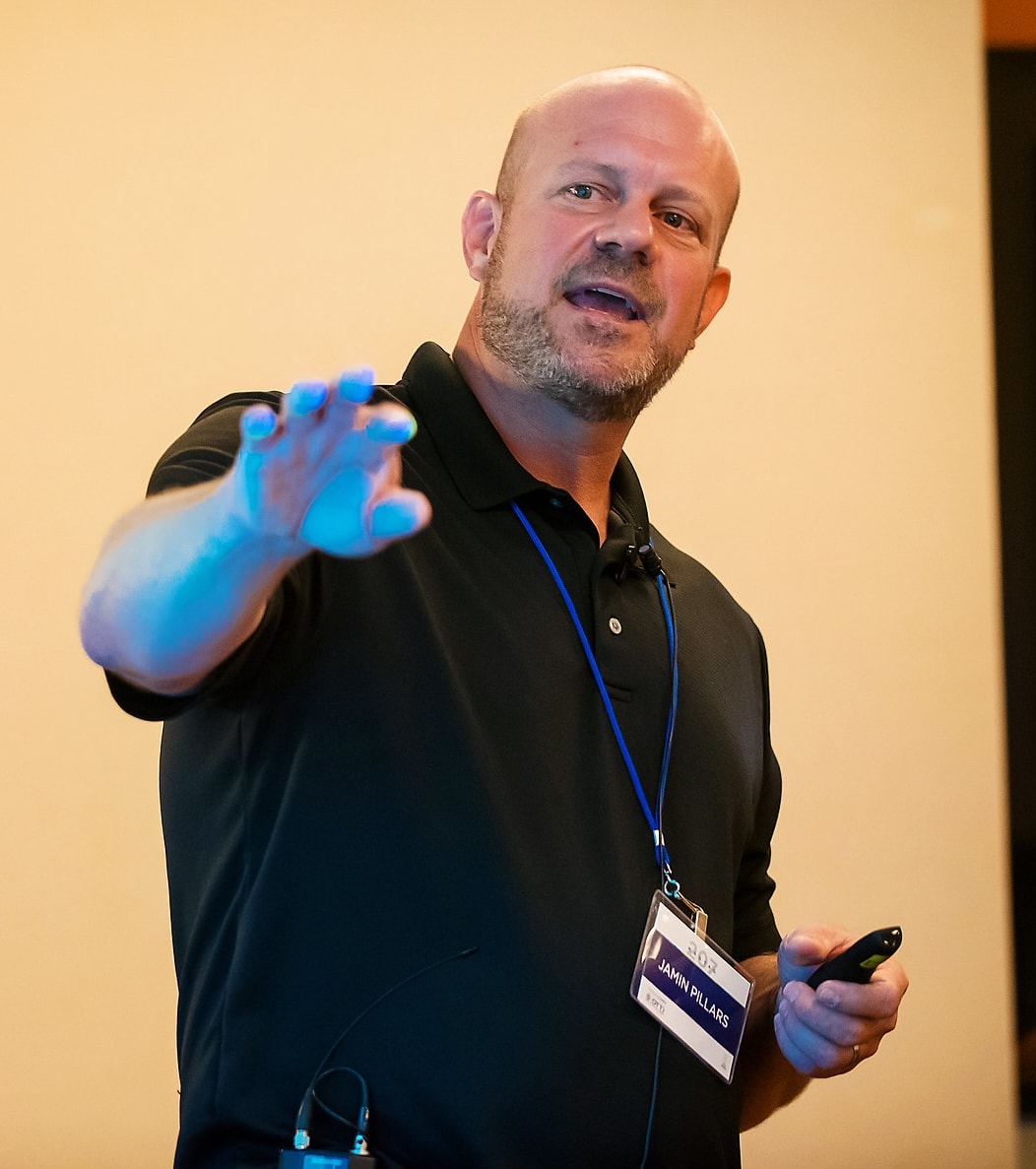
Dr. Jamin Pillars
- 14 years at Sandia as a Principal Member of Technical Staff; led the Magnetic Smart Tags (MaST) program for NNSA
- Ph.D., University of New Mexico, electrodeposition of high-magnetostrictive CoFe alloy films
- Focus: magnetoelastic MEMS, batteryless sensing in RF-denied environments, through-barrier phononic communication
- Named inventor on 5 issued U.S. patents (assigned to Sandia), with 3 pending

Christian L. Arrington
- 25 years on research staff across MEMS/NEMS and precision microfabrication for DOE, NNSA, DARPA, IARPA, and DTRA
- M.S., Materials Engineering, New Mexico Tech; B.S., Chemistry, University of New Mexico
- Focus: LIGA and high-aspect-ratio lithography, electroforming, MEMS/NEMS, superconducting and quantum devices
- Named inventor on 8 issued U.S. patents (assigned to Sandia) in microfabrication and electrodeposition
Foundational IP developed at Sandia National Laboratories: US 10,132,699, US 10,215,648, US 10,260,969, and US 10,510,945.
Design, fabrication, and characterization happen under one roof, in VastVision's own cleanroom and microfabrication facility in Albuquerque.
Have a program that needs this material?
Bring us the geometry, the frequency, or the environment. We'll scope the deposition.