Quantum · with NIST
Electroformed ion traps
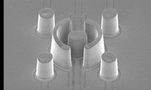
Gold ion-trap electrodes for quantum computing research: 80 µm posts standing 150 µm tall, alongside 3 µm thick gold features and 10 µm lines.
We fabricate thick, high-aspect-ratio, uniform metal and metal-alloy structures that are too small for traditional machining, using LIGA-style lithography and void-free, bottom-up electroforming.
Our metal micromachining program specializes in high-aspect-ratio micromachining (HARM): tall, narrow, precise metal and metal-alloy structures that fall below the reach of conventional machining. Rather than removing material, we grow it, following the LIGA sequence of lithography, electroforming, and molding: thick-resist molds with near-vertical sidewalls, bottom-up electroforming, and precision planarization. That geometry packs more strength, surface area, and conductivity into less space, for demanding applications across quantum, energy, RF, and medical imaging.
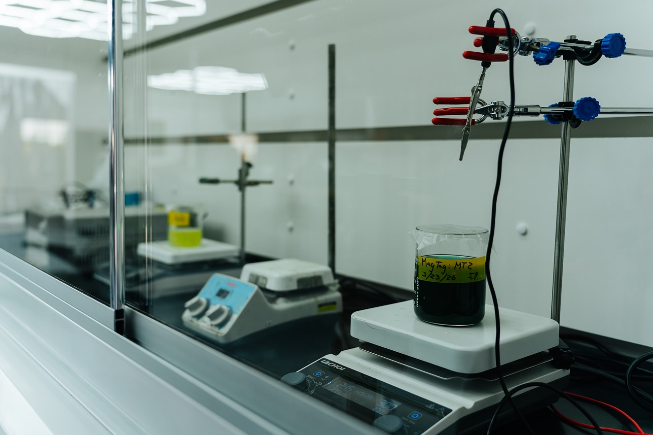
Electrochemistry R&D is the basis for dense, uniform, high-aspect-ratio metal: new and refined deposition chemistries, bath control for grain structure and stress, and characterization to validate every result.
Dedicated labs for lithography, electroforming, and planarization let us iterate quickly on mold geometry, plating parameters, and finishing, and calibrate for fidelity across a wafer.
We deliver finished, functional hardware: metal and metal-alloy coatings and high-aspect-ratio 2.5D electroformed structures too fine for conventional machining.
Our process follows LIGA (Lithographie, Galvanoformung, Abformung: lithography, electroforming, molding), using UV light and thick SU-8 or PMMA resists in place of synchrotron X-rays. Three tightly coupled steps take a design from mask to finished, characterized part.
A precise photoresist mold is built on a conductive seed layer. UV exposure transfers the device geometry into a thick resist, defining near-vertical sidewalls for the metal to grow within.
Metal is grown from the bottom up, not machined from the top down. Superfill chemistry makes deposition fastest at the bottom of each cavity, so deep, narrow features fill solid with no trapped voids or seams.
Overplated metal is lapped and polished flush with progressively finer diamond media. The resist is then stripped to leave free-standing microparts, or the structure is kept as a mold insert for replication.
Our process comes out of Sandia National Laboratories’ Metal Micromachining Team (MMT), where VastVision research scientist Christian Arrington spent years electroforming gold, copper, and indium microstructures for Sandia programs and outside collaborators including NIST and NASA.
That work is the foundation of the lithography, electroforming, and planarization process we run today.
Work performed by Sandia’s Metal Micromachining Team. Images courtesy of Sandia National Laboratories.
Quantum · with NIST
Gold ion-trap electrodes for quantum computing research: 80 µm posts standing 150 µm tall, alongside 3 µm thick gold features and 10 µm lines.
2007 to 2010
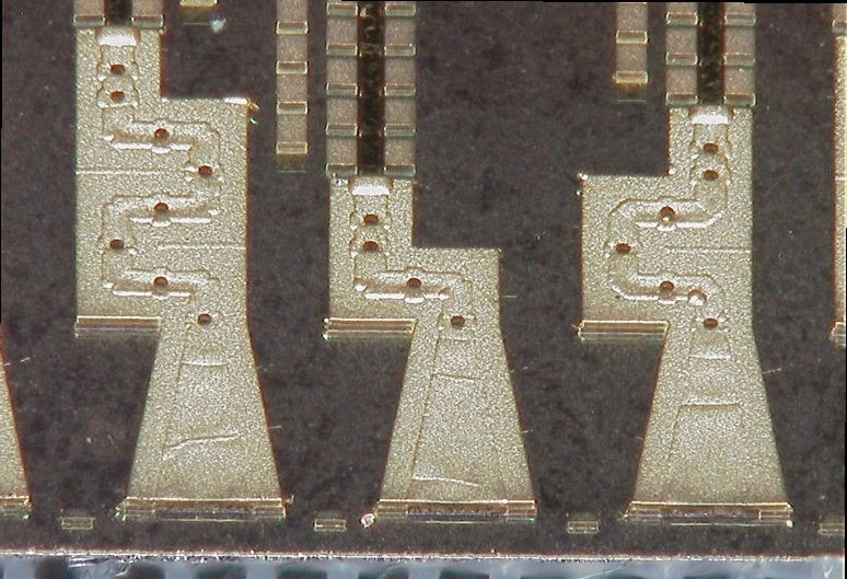
Multilayer gold waveguides electroformed directly on 10 µm tall terahertz quantum cascade lasers, with no planarization needed. On-chip beam control of the laser was demonstrated.
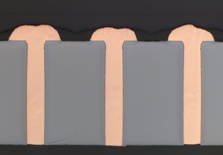
2011 onward
Void-free, full-thickness copper fill of DRIE silicon, hermetic to 10⁻¹¹ atm·cc/s helium with leakage below 15 pA. The same approach filled vias in alumina, sapphire (platinum), and photo-defined glass (through-glass vias).
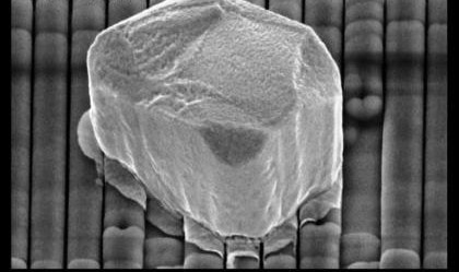
2008 to 2012
A pulse-plating process taken to TRL 5: 13 µm/hr deposition with ±1 µm uniformity, aligned bonding of 4 µm bumps at 8 µm pitch, sub-micron bumps, and hardware delivered to NASA.
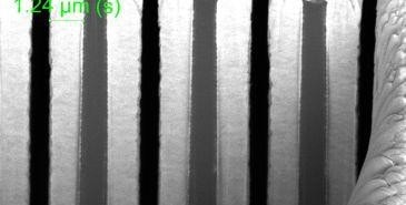
High aspect ratio
Low-stress gold plated 1 µm thick and fully conformal over silicon gratings with a 35:1 aspect ratio, reaching the base where CVD tungsten could not. Gratings up to 50 µm tall have been plated.
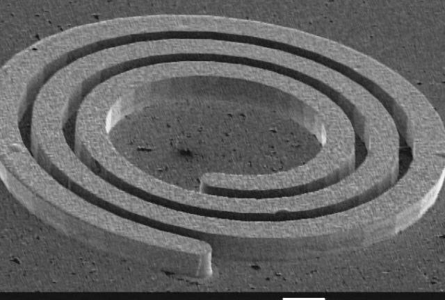
Electroformed coils
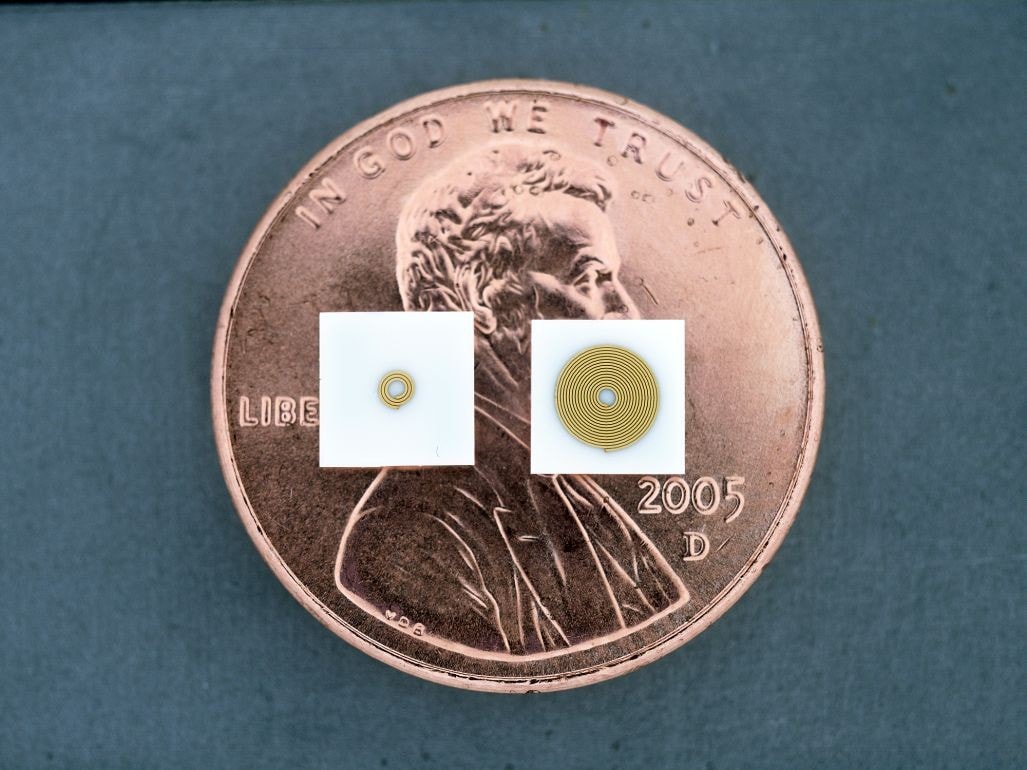
Spiral and rectangular gold coils small enough to sit side by side on a penny, with electroformed backside contacts through filled vias.
Three dedicated laboratories carry a build from lithography through electroforming to final finish, with in-line metrology at every stage.
Class 100 cleanroom for mold definition and resist processing.
Electroforming plus in-line metrology to verify every build.
Precision finishing to final tolerance.
Our metal micromachining capabilities support advanced programs including:
Tell us which capabilities you need and a bit about your part. A VastVision engineer will walk you through how our lithography, electroforming, and planarization labs apply, and follow up within one business day.