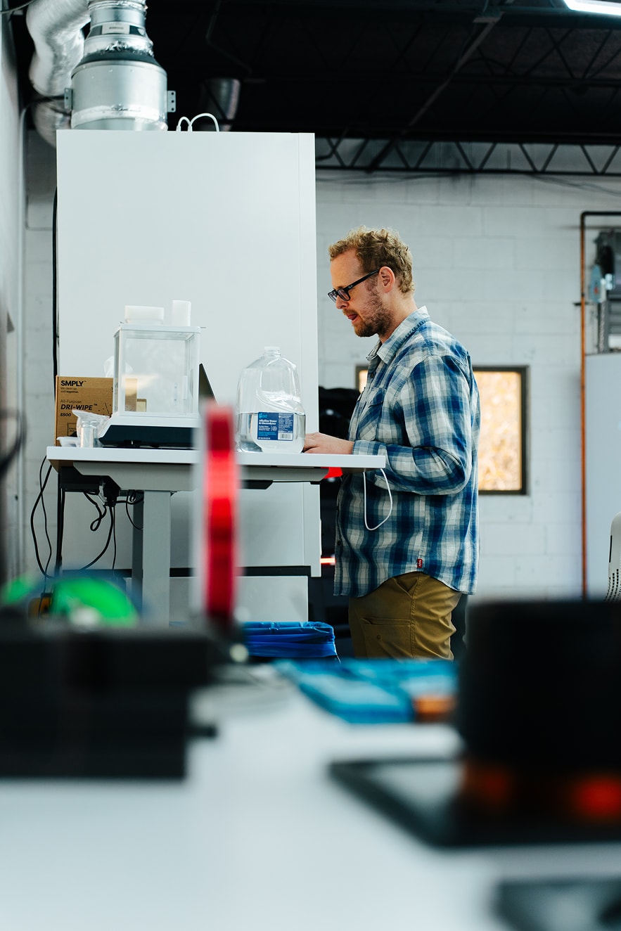
Stop 01
Microfabrication
Our Class 5 cleanroom and process tools, where thin films and MEMS devices are patterned, deposited, etched, and released.
Class 5 cleanroomUV lithographyPlasma etch
Learn more →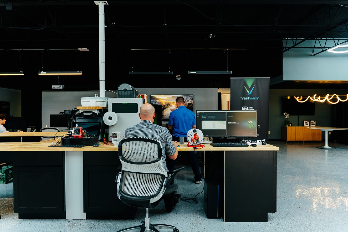
Walk the cleanroom, watch the electron microscope work, and meet the scientists behind our research. Tours are guided, small, and built around what you’re working on.
We design, fabricate, and test under one roof, so a tour follows the path an idea takes here: from a film on a wafer to a sensor on the bench.
Our Class 5 cleanroom and process tools, where thin films and MEMS devices are patterned, deposited, etched, and released.
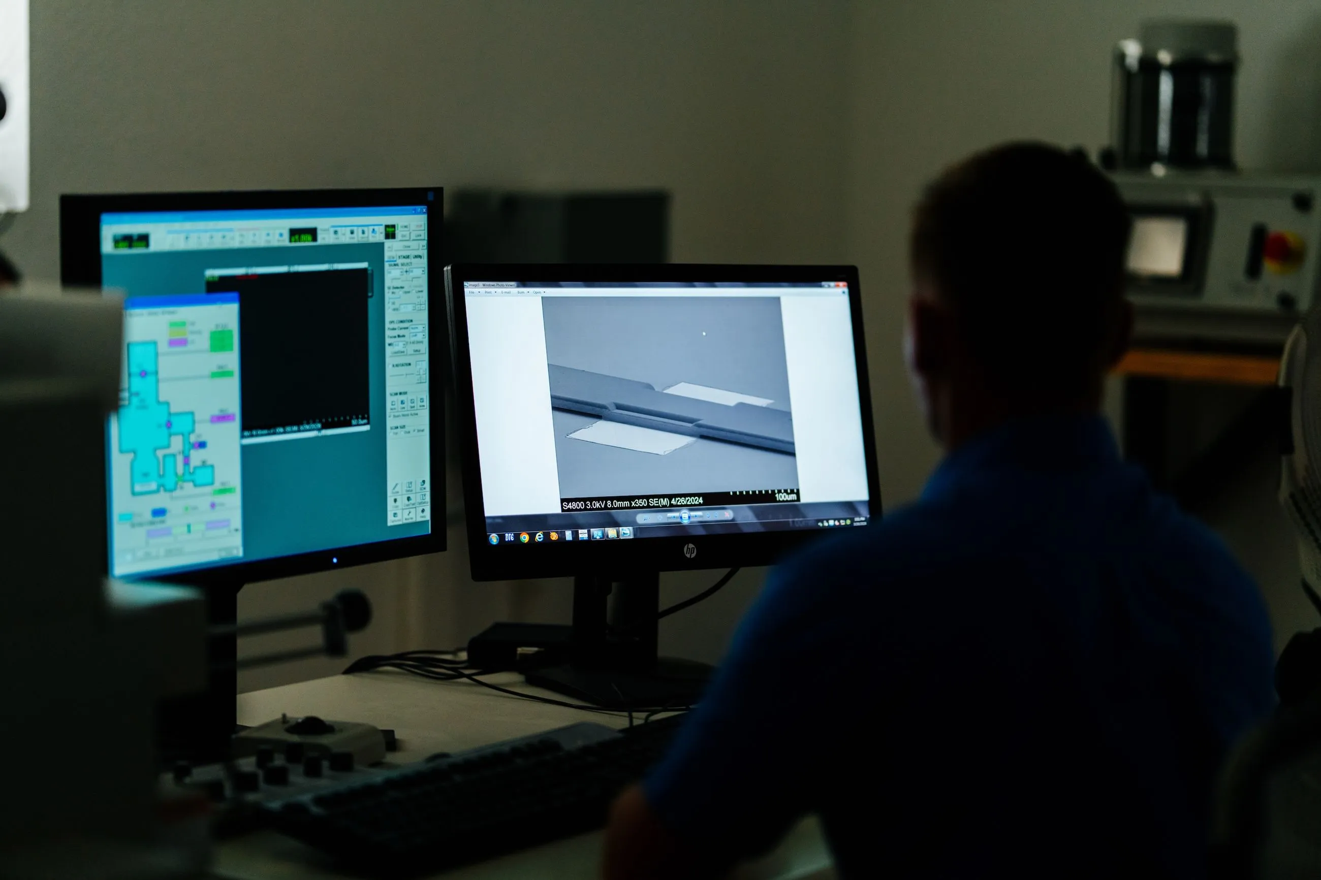
Our field-emission SEM, imaging to the nanometer scale and mapping what a sample is made of.
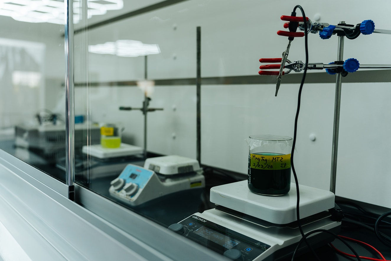
Where our materials research happens: electrodeposition, coatings, and the finishing line that turns them into parts.
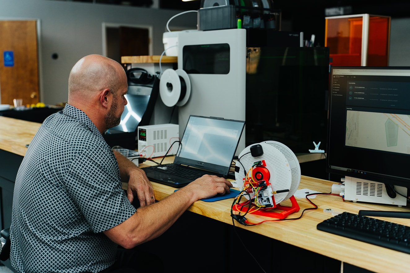
Sensors and boards come together here, from first bring-up to the hardware we put in the field.
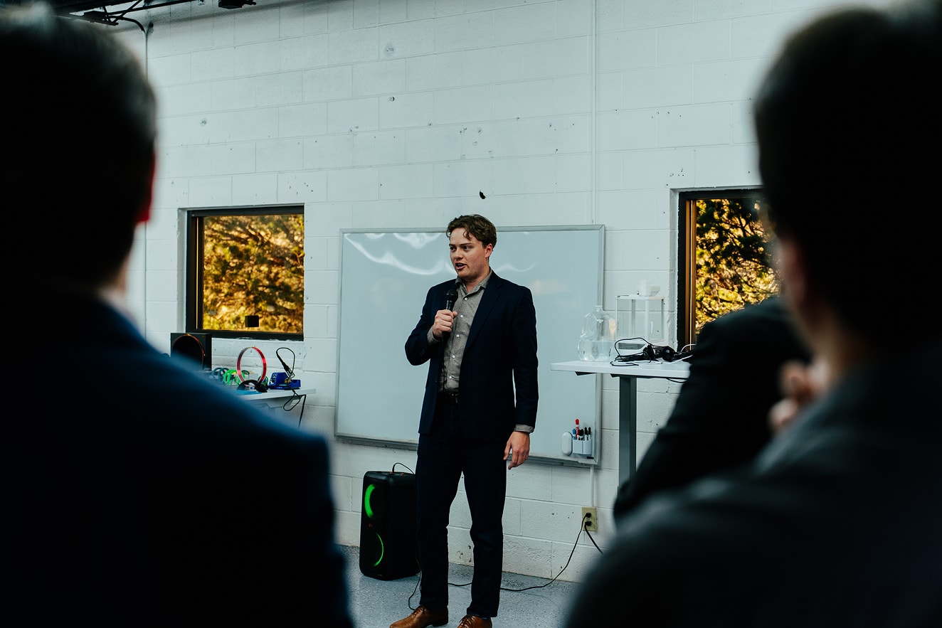
No sales tour. You’ll walk the lab with our scientists and engineers, and the conversation goes wherever your problem takes it.
Tell us when you’d like to come and what you want to see. We’ll reply within one business day to confirm.